-
10 Hardest Bosses in Crimson Desert
Crimson Desert is an open-world action-adventure game from Pearl Abyss that throws players into the war-torn world of Pywel, where fast, brutal combat is a huge part of the experience. Whether you are pushing through the main story or wandering off the path to test yourself against stronger enemies, the game makes boss fights feel like a major part of the journey.
In total, this article looks at 76 bosses, including 25 main story bosses and 51 optional bosses, and the hardest ones stand out because they demand sharp timing, patience, and a real understanding of how the combat system works. The game follows Kliff across Pywel, and official materials describe it as an open-world action-adventure title centered on his journey through a dangerous fantasy continent.
10. Kearush the Slayer
Kearush the Slayer earns a place on this list because he is one of the first bosses in Crimson Desert that can truly overwhelm unprepared players. Encountered at Hernand Castle during Act 5, Kearush is a mandatory main story boss, and the fight is made even tougher by his three full health bars. That alone turns the battle into a long test of patience, consistency, and resource management.
What makes Kearush especially dangerous is how much pressure he puts on the player at all times. He uses wide, heavy attacks such as ground slams, grabs, body drops, and wall-climbing leap attacks, and his aggression increases as the fight goes on. Because of that, players cannot simply trade damage with him. They need to manage Spirit carefully, avoid panic dodging, and wait for safe openings instead of getting greedy.
Kearush does have weaknesses. Fire damage can knock him down and create valuable damage windows, and the mounting system gives players another way to wear him down. Still, those mechanics do not remove the challenge. They just make the fight more manageable for players who understand how the boss works. It is also worth noting that Kearush was harder before later balance changes, so players who beat the pre-nerf version deserve credit for taking down a much tougher early-game skill check.
9. The Reed Devil
The Reed Devil does not overwhelm players through size. He does it through uncertainty. Encountered on Frozen Soul Mountain during the Chapter 3 main quest “Dance with the Devil,” this mandatory boss turns a sword fight into a stalking match. He slips into the reeds, disappears from view, and attacks from sudden angles, which makes the arena itself part of the challenge. Instead of tracking a large target in open space, players have to read movement in the grass, dust plumes, and brief visual tells before the next strike lands.
That is what gives the fight its identity. The Reed Devil is fast, lightly built, and far more evasive than most of the game’s early bosses. His pressure comes from quick sword attacks, smoke-like repositioning, knife throws, and unblockable moves such as Swift Stab and Overhead Stab. The danger is cumulative. He does not need one huge hit to break the player down because he is constantly forcing defensive reactions, draining stamina, and resetting the pace before players can fully settle in.
Then the fight adds a second layer. After the first phase, the player has to destroy five totems while ignoring the boss’s duplicates, which briefly turns the encounter from a duel into a survival scramble. Once Phase 2 begins, he keeps his earlier tricks but becomes more aggressive and gains new unblockable wave attacks. That shift is a big reason he belongs on this list. The Reed Devil is not the largest or most cinematic boss in Crimson Desert, but he is one of the most disruptive because he forces players to fight on his terms from start to finish.
8. Fortain, the Cursed Knight
Most boss fights ask one question: can you handle the boss in front of you? Fortain asks three at once. By the time Kliff reaches him at the end of a fortress siege, the fight is no longer a clean duel. Fortain is already dangerous on his own, but the real problem is everything happening around him. He fights in heavy armor with a cursed sword and shield, his spectral summons attack on their own timing, and soldiers around the fortress keep firing projectiles into the arena. That layered pressure is what makes Fortain feel harder than a normal human boss.
His shield is the reason the battle becomes so chaotic. It can summon spectral beings that act independently of Fortain’s own attacks, which means players are often tracking overlapping threats instead of reacting to one clear pattern. One moment Fortain is closing distance with a shield charge or sword strike, and the next a ghostly melee or ranged attack is arriving on a separate rhythm. That makes spacing, stamina control, and awareness much more important than raw aggression.
The setting matters too. This fight takes place during a siege, and the fortress soldiers are not just background detail. Their shots can interrupt attack windows and punish players who tunnel vision on Fortain himself. That is a big part of why this encounter stands out. Fortain is not the fastest or strangest boss in Crimson Desert, but he is one of the most oppressive because the player is never dealing with just one enemy. The fight turns crowd pressure into the main mechanic, and that makes it memorable for all the wrong reasons.
7. Crimson Nightmare
Crimson Nightmare is difficult for a simple reason: the fight stops being a normal boss fight almost immediately.
Found at Fort Perwin as part of the House Roberts questline, this optional boss is built around a mechanic that can confuse players the first time they see it. The boss floats inside a protective cube, sits in the middle of the Crimson Fog, and cannot be beaten by running in and swinging like usual. The fog constantly drains health, inflicts Confusion, and turns the whole arena into a hazard even before the boss itself starts attacking.
That design is what makes Crimson Nightmare memorable. Many bosses in Crimson Desert test timing or dodging. This one tests whether the player understands the fight at all. Physical attacks do very little while the barrier is active, so the real answer is using Force Palm, Focused Repulsion, or other stagger tools to break the boss’s protection and expose its core. Once the core drops, the fight suddenly becomes manageable, but only for a short damage window before the whole cycle starts again.
The preparation also matters more here than in many other encounters. A fog-immunity mask such as the Scarlet Blades Gas Mask can completely change the experience, and Focus management is just as important as health because running out of Spirit means losing your main way to stagger the boss. That gives Crimson Nightmare a very different kind of difficulty. It is not one of the hardest bosses because it is the most aggressive or the most powerful. It earns its place because it punishes players who do not understand its system, and that makes it one of the game’s most unusual early skill checks.
6. Antumbra’s Staff
Miss the interrupt, and this fight can go bad in a hurry.
Antumbra’s Staff guards the Sanctum of Solace during the Witches Faction Quest, southwest of the City of Pailune, and the encounter is built around one mechanic more than any other: a charged ground slam that has to be stopped with Force Palm. The boss is not especially complex on paper, but that is exactly why it is dangerous. Once the player understands the pattern, the fight becomes manageable. Until then, the damage can feel punishing.
That single attack defines the entire battle. When Antumbra’s Staff begins charging energy into its weapon, players have only a short window of about two to three seconds to react. A successful Force Palm interrupt cancels the slam and leaves the boss stunned, creating a clean opening for damage. If the interrupt fails, the attack lands as a large area hit that deals heavy damage and is not meant to be safely blocked. That turns the fight into a test of recognition and execution rather than raw aggression.
The rest of the moveset exists to make that timing harder. Antumbra’s Staff mixes in sweeps, quick strike chains, and overhead attacks, which means players have to stay close enough to interrupt the slam without getting trapped too close to the boss’s regular pressure. Its official combat stats also show that this is not a lightweight enemy, with 4,116 health, 265 attack, and a knockout threshold of 750. That gives the fight enough durability and damage to punish mistakes, even if the central gimmick sounds simple.
What earns Antumbra’s Staff a place on this list is how cleanly it turns one mechanic into a real skill check. Some bosses overwhelm with chaos. This one is more disciplined than that. It asks a direct question over and over: can you read the charge-up, close the distance, and interrupt on time? If the answer is no, the fight quickly becomes much harder than it first appears.
5. Antumbra’s Spear
On paper, Antumbra’s Spear does not look like one of the nastiest bosses in Crimson Desert. It shares the same 4,116 health, 265 attack, 100 defense, and 750 knockout threshold as Antumbra’s Staff, and its patterns are described as fairly repetitive once you learn them. The problem is that repetition does not always make a boss easy. In this case, it makes the fight punishing in a very specific way, because the spear’s reach, the boss’s mix of physical and magical attacks, and the added pressure of surrounding enemies create a rhythm that keeps catching players who read the wrong move at the wrong time.
That mixed offense is the real headache. Antumbra’s Spear can pressure players with thrust combos, sweeping strikes, a ground slam, and a charge lunge, but it also throws out magic projectiles that cannot be blocked or parried. So the fight is constantly asking a small but important question: do you need to parry this, or do you need to dodge it? Get that answer wrong, and the damage starts stacking fast. The spear’s long reach makes that even worse, because backing away is often less safe than moving to the side.
There is also no clean one-on-one comfort here. The Sanctum of Revelation includes other Antumbra enemies, including floating sphere foes and cultists, which means the fight can become messy if players do not thin the area out first. Even when the boss itself feels readable, the extra enemies add chip damage and distraction, and that matters in a fight built around reaction timing.
Antumbra’s Spear is beatable with a solid plan. Force Palm can stun it for several seconds, especially during the ground slam wind-up, and physical attacks can be parried into heavy counters. But that does not make the encounter soft. It earns this spot because it punishes hesitation, punishes the wrong defensive choice, and turns a seemingly straightforward mid-tier boss into a fight that feels much harsher in practice than it first appears.
4. Beloth the Darksworn
Beloth the Darksworn is where Crimson Desert stops asking for clean execution and starts demanding full preparation. Found at Hoenmark Ruins in Hernand, this optional world boss appears during the “Wraith in the Frost” quest in the White Blizzard line, and the fight is built around brutal environmental pressure as much as direct attacks. Even before Beloth’s halberd starts swinging, the arena is already working against the player through constant cold damage, freeze effects, and stamina lockouts that can leave Kliff unable to dodge at the worst possible moment.
The numbers help explain why the fight has such a reputation. Beloth has 13,000 HP, 450 attack, and a knockout threshold of 1,000, which gives him far more staying power than many earlier bosses. He also belongs to the game’s Overwhelming Beings tier, and the encounter backs that up with attacks that punish bad habits immediately. His ice flurry can end in a frost slam that passes through pillars, his spear throw can kill players outright if it connects cleanly, and his teleport strike exists mainly to punish anyone who tries to play too far away.
What makes Beloth especially nasty is that the fight is not just about dodging on reaction. Players have to understand how the arena works. Pillars can block the spear throw but not the ice slam. Ice resistance is effectively mandatory just to survive the room. Fire damage is his major elemental weakness, but even with that advantage, the fight still demands patience because greed gets punished fast. The safest approach is usually slow, controlled chip damage, careful cover use, and knowing exactly which finisher Beloth is about to use before committing to a punish.
That is why Beloth belongs this high on the list. He is not hard because he is messy. He is hard because nearly every part of the encounter is designed to squeeze the player at once: the weather, the arena, the resource drain, the one-shot threat, and the punish windows that only open if you read the pattern correctly. By the time most players beat him, they have usually stopped trying to overpower the boss and started learning how to survive him.
3. Antumbra’s Sword
Antumbra’s Sword is probably the point where the Antumbra fights stop feeling like regular sanctum bosses and start feeling like real wall fights. Located in the Sanctum of Absolution in southwest Hernand, this boss uses the same basic stat line as the other Antumbra variants at 4,116 health, 265 attack, 100 defense, and a 750 knockout threshold, but it is much more dangerous in practice because of how fast and aggressive its moveset is.
The main problem is how little downtime the fight gives you. Antumbra’s Sword teleports, reappears from black mist, chains melee attacks quickly, summons mirror images, and fills the arena with dark energy waves. That pressure makes the fight harder than Antumbra’s Spear or Antumbra’s Staff, because players are not just reacting to one weapon. They are dealing with movement, clone attacks, unblockables, and projectile coverage at the same time. Underprepared players can get dropped in a couple of hits, and some of the illusion-based attacks can effectively one-shot if the timing goes wrong.
This is also one of those fights where the answer is not to play more aggressively. In fact, that usually gets players killed. The safest approach is short punish windows, careful stamina management, and using the right tools at the right time. Focus Level 3 is described as especially important because it slows time enough to make the boss’s speed more readable, while Blinding Flash can interrupt some of the most dangerous attacks, including the ground thrust that sends sword waves across the arena. There is also a pillar near the edge of the arena that can absorb some of the projectile waves when skills are on cooldown.
That is why Antumbra’s Sword ranks this high. Its raw stats do not look outrageous compared with the other Antumbra bosses, but the fight itself is much less forgiving. It is faster, more chaotic, and much more likely to punish overcommitting. By the time most players beat it, they have usually learned the same lesson: against this boss, discipline matters more than damage.
2. Ator, Archon of Antumbra
Ator feels like the final exam for the Antumbra side of Crimson Desert. He waits at the bottom of the Cloister of Ruination in western Pailune, and players cannot reach him until they have beaten Antumbra’s Sword, Antumbra’s Spear, and Antumbra’s Staff. Unlike several other hard fights in the game, this one strips away distractions. There are no adds to clean up and no easy way to cheese the encounter. It is just Kliff against a world boss with 11,000 HP, 800 attack, and a 1,000 knockout threshold.
What makes Ator so hard is not just the damage. It is the way the whole fight forces discipline. He throws out orb projectiles that are dangerous to block, mixes in sword strings with a fake-out fourth slash, uses hammer attacks that can almost erase you if they land cleanly, and can enter a darkness phase that drops visibility and forces players to track his position by the glow of the hammer. He also has an invincibility shield state, which means players cannot just stay aggressive all the time. They have to know when to stop attacking and reset.
This is also a fight where normal chip damage is not enough. Ator’s defense is high enough that the real progress comes from stagger windows, not random hits. The guide’s recommended approach centers on landing full combo strings, managing Spirit carefully, and cashing in when he finally staggers. That makes the fight feel longer and heavier than many bosses with flashier mechanics. If the player gets impatient, wastes stamina, or guesses wrong on one of his punish windows, the run can fall apart fast.
That is why Ator belongs near the very top of this list. He is not just a strong boss. He is a boss built to punish weak habits. By the time players beat him, they usually are not winning through brute force. They are winning because they finally learned when to attack, when to back off, and how to survive long enough to make the stagger windows count.
1. The Forgotten General
For the top spot, it comes down to one mechanic: illusions. The Forgotten General is fought in the General’s Tomb at the northwestern point of Silver Wolf Mountain, west of ODC, and the encounter does not unlock until the full Pailune questline is complete. A cited guide gives her 13,000 HP and 480 attack, which already puts her in top-tier boss territory before the actual gimmick even starts.
What makes the fight worse than the others is that her attacks do not end when they look like they should. Partway through many of her spear strings, she spawns an illusion that repeats or extends the attack, so a normal dodge timing can suddenly become wrong. That is why this fight is often described as the hardest among the Overwhelming Beings. The boss technically can be parried, but the illusion follow-ups break that rhythm so often that relying on parries becomes much riskier than usual.
There is also very little relief built into the encounter. The fight is mostly a straight skill duel at medium range, with no easy projectile-based answer and no simple way to slow the pace down. One of her key punish windows comes after a combo that ends in a leap slam, but even then the player has to stay disciplined and avoid attacking into her guarded spear stance, since that can lead directly into a parry and counter sequence. At certain points she also disappears and sends waves of illusions across the arena, forcing players to either use a known safe corner or go airborne with Pogo Palm and Aerial Roll to avoid getting run over.
That is why the Forgotten General works as the No. 1 pick. Other bosses hit harder in specific moments or require more setup, but this one puts the most pressure on pure reaction, spacing, and consistency. The illusion system keeps turning familiar openings into traps, and that makes the whole fight feel less stable than the others. When players say this is the hardest boss in Crimson Desert, that judgment makes sense.
Conclusion
Crimson Desert does not hold back when it comes to boss design. Across its 76 total bosses, the toughest fights stand out because they test different parts of the player’s skill set, whether that means timing, patience, spacing, preparation, or the ability to stay calm when a fight starts to fall apart. The hardest bosses in the game are memorable not just because they hit hard, but because they force players to learn, adjust, and eventually win on the game’s terms.
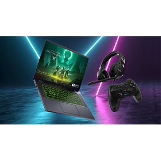
If you are planning to take on brutal fights like these on PC, having the right hardware helps. Acer’s best budget laptop for gaming, the Nitro V 16 AI, is a strong option for players who want smooth performance without jumping straight into the premium tier. It combines Windows 11 Home, an AMD Ryzen 7 350 processor, NVIDIA GeForce RTX 5060 graphics with 8 GB of dedicated memory, 16 GB of DDR5 RAM, and a 1 TB SSD, along with a 16-inch WUXGA 180 Hz display that gives fast-moving action more clarity. You can also learn more about the model on Acer’s item page.
For players who want to push even higher settings, faster frame rates, and more demanding visual presets, the premium gaming laptops from the Acer Predator lineup is worth a look as well.
Recommended Products
Acer Nitro V 16 AI (RTX 5060)
Buy Now
Predator Helios Neo 16 AI
(RTX 5070Ti) Buy Now
Acer Nitro 85 (RTX 5070)
Buy Now
-
Are RAM Prices Finally Dropping?
Highlights
RAM prices are starting to drop in some retail markets, but the broader memory shortage is not over. AI and server demand are still putting pressure on supply, so prices may remain high or rise again later in 2026. For most buyers, the best move is to avoid panic buying, watch for deals, and choose a laptop or desktop with enough RAM built in if they already need an upgrade.
RAM prices are finally giving buyers a little breathing room, but breathing room is not the same as relief. After a brutal 2025, when DDR4, DDR5, LPDDR5, and server memory all became more expensive as AI demand pulled supply away from consumer hardware, some retail RAM prices have started to flatten or even dip in select markets. That sounds like good news for PC builders, laptop shoppers, and gamers, but the larger memory market has not returned to normal. DRAM contract prices are still projected to rise sharply in Q2 2026, suppliers are still prioritizing AI and server demand, and analysts warn that the recent retail drop may be a short-term correction rather than the end of the RAM crisis.
Why the RAM crisis happened
The RAM crisis started because memory demand changed faster than memory supply could respond. For years, consumer RAM was treated as a predictable PC component. Then AI data centers began competing for the same broader memory supply chain, especially high-bandwidth memory, or HBM, which is used in advanced AI accelerators. As suppliers shifted more wafer capacity, packaging resources, and long-term contracts toward server and AI customers, less capacity was left for ordinary DDR4, DDR5, LPDDR5, SSDs, and other consumer-facing memory products. That is why the price shock has not been limited to DIY RAM kits. It has also affected laptops, desktops, phones, game consoles, and storage devices.
The problem is not simply that manufacturers can “make more RAM.” Memory production depends on expensive fabs, limited 300 mm wafer supply, advanced packaging capacity, and long planning cycles. New plants can take years to build and ramp to volume production, which means suppliers cannot quickly flood the market with more DRAM just because prices are high. SK Hynix, for example, has invested heavily in advanced packaging for AI memory, but that still reflects the same reality: the fastest-growing demand is coming from AI infrastructure, not consumer PC upgrades.
There is also a product mix issue. DDR4 was already being phased down as the industry moved toward DDR5, while HBM and server memory became more attractive to manufacturers because data center customers are willing to pay more and sign larger long-term contracts. At the same time, modern devices are using more memory than before. Many laptops now ship with 16 GB or 32 GB, games and creative workloads are more demanding, and AI features are increasing memory requirements across PCs and mobile devices.
That is why the RAM crisis became so severe. It is not one shortage in one category. It is a supply chain being pulled toward higher-margin AI, server, and enterprise customers while consumer demand remains high. Even with new investment, the market remains tight, and consumers are still competing against buyers with deeper pockets and larger long-term contracts.
Are RAM prices finally starting to go down?
Some RAM prices have started to come down, but buyers should be careful about what that really means. The recent price drop is real in certain retail markets, but it needs context. German consumer RAM prices reportedly fell 7.2% month over month, while Chinese retail pricing was down 20%. One U.S. example also showed a 32 GB Corsair Vengeance DDR5 kit falling from $490 to $380, a drop of about 22%. That sounds encouraging, especially after months of brutal price hikes.
But these discounts are coming from extremely elevated prices, not from normal market conditions. Earlier in the crisis, some DDR5 modules had already climbed 120% to 200%, while broader DRAM pricing indexes were up nearly 50%. In other words, a 7%, 20%, or even 22% drop does not erase the larger surge that came before it. RAM may be cheaper than it was a few weeks ago, but it is still far more expensive than it was before the crisis.
The more likely explanation is that retailers and resellers pushed prices too high, then had to pull back when consumers slowed their purchases. The market may be correcting the most aggressive retail pricing, not fixing the underlying shortage. Some of the recent softness may come from localized inventory pressure, weaker consumer demand, or stores trying to move stock before the next round of supply-chain increases reaches retail shelves.
That distinction matters. A true recovery would mean that the supply side has meaningfully improved. That has not happened yet. The same supply pressures are still in place, even if some retail prices have softened. AI and server customers continue to command much of the industry’s attention, and consumer RAM remains exposed to the same tight market that caused prices to surge in the first place.
So will this downward trend continue? Probably not in a meaningful way. Short-term discounts may continue to appear, especially on specific RAM kits or during retail promotions, but the broader trend still points toward elevated pricing. More importantly, the contract market still points upward, with TrendForce expecting conventional DRAM prices to rise another 58% to 63% in Q2 2026. That suggests the recent dip may be more of a temporary pause than the start of a full price recovery.
For consumers, that means RAM may feel slightly less painful to buy than it did a few months ago, but the market is still far from cheap. The current drop is better understood as a correction after an extreme spike, not a sign that the RAM crisis is over.
Will RAM prices go up again later?
The recent drop may not last. If today’s lower retail prices are mostly a short-term correction, RAM could become more expensive again as higher supply-chain costs move through the market.
That is the key point for consumers: retail prices and contract prices do not always move at the same time. A store may lower prices to clear inventory or attract buyers after demand slows, even while manufacturers and large buyers are still negotiating higher prices behind the scenes. If those higher costs reach retailers later, today’s discounts could disappear quickly.
Efficiency gains in AI may not solve the problem either. Google’s TurboQuant technology reportedly claims up to 6x lower memory usage for AI models, which sounds like it should reduce pressure on the memory market. But if AI companies are still compute- and memory-constrained, using memory more efficiently may simply let them run more models, process more requests, or expand workloads instead of releasing supply back to consumers.
That is why the recent price dip should not be treated as a return to the old pricing environment. It may help buyers who already planned to upgrade, but it does not prove that the shortage is over. Unless supply expands faster than expected or AI demand cools sharply, RAM prices are likely to remain expensive, uneven, and vulnerable to another round of increases.
What should consumers do now?
For most consumers, the smartest move is to buy based on need, not panic. If your current laptop or desktop still handles your daily work, school, gaming, or creative tasks comfortably, there is no need to rush into an upgrade just because RAM prices may rise again. Paying more for memory you do not need yet is still paying more.
But if your system is already struggling, waiting for a full return to old RAM prices may not be realistic. The market has softened in some places, but the larger supply chain remains under pressure. If you need more memory for gaming, video editing, AI tools, schoolwork, remote work, or general multitasking, this may be a reasonable time to compare prices and buy when you see a configuration that fits your budget.
One practical option is to look at complete systems instead of upgrading piece by piece. Pre-configured laptops and desktops can sometimes offer better value because the memory, processor, graphics, display, and storage are already balanced for the intended use. That can be especially helpful in a market where individual RAM kits may swing sharply in price.
For everyday users, students, professionals, and remote workers, the Acer Swift lineup is worth considering. Swift laptops are built around portability, productivity, and efficient performance, making them a strong fit for users who want a thin and light laptop that can handle modern multitasking without feeling bulky. Choosing a system with enough memory from the start can also reduce the need for expensive upgrades later.
For gamers and creators, the Acer Nitro lineup is a strong fit for users who want solid performance without overspending. Nitro laptops and desktops are built to deliver a good balance of graphics power, fast displays, memory, and storage at a more accessible price point than premium gaming systems. That makes them especially practical for modern games, streaming, school projects, entry-level content creation, and everyday multitasking. In a volatile RAM market, buying a complete Nitro system with a balanced CPU, GPU, and memory configuration can be a better bang-for-your-buck option than building or upgrading one component at a time.
The main takeaway is simple: the RAM crisis may be easing at retail, but it is not over. Do not buy out of fear, but do not assume prices will quickly return to where they were before the surge. If your current device still works well, wait and watch for better deals. If you already need an upgrade, focus on total system value, choose enough memory for the next few years, and consider a well-configured Acer Swift or Nitro system before component prices rise again.
Readers who want to better understand RAM, upgrades, and memory management can also check out our related guides. Learn how to clear RAM in Windows 11, follow our step-by-step guide to upgrading your Acer laptop’s RAM, or explore Acer computers with 32 GB or more of RAM if you are considering a system with more memory from the start.
FAQ
Are RAM prices going down?
Some RAM prices have started to fall in certain retail markets, but that does not mean the RAM crisis is over. The recent drop appears to be a short-term correction after months of steep price increases, not a full return to normal pricing.
Why did RAM prices get so expensive?
RAM prices rose because AI data centers began consuming more memory supply, especially high-bandwidth memory used in advanced AI hardware. At the same time, manufacturers shifted more capacity toward server and AI customers, leaving less supply for consumer products like laptops, desktops, gaming PCs, phones, and RAM kits.
Will RAM prices go back to normal soon?
Probably not soon. Memory production takes years to expand, and demand from AI, data centers, and modern consumer devices remains high. Short-term discounts may appear, but a broad return to pre-crisis RAM prices is unlikely in the near future.
Could RAM prices go up again?
Yes. The recent retail drop may not last if higher contract prices and supply-chain costs move through the market. If retailers are only lowering prices to clear inventory or attract buyers, prices could rise again once new costs reach store shelves.
Should I buy RAM now or wait?
Buy based on need, not panic. If your current device still performs well, it may be worth waiting for deals. But if your laptop or desktop is already struggling with gaming, multitasking, creative work, or AI tools, waiting for much lower RAM prices may not be realistic.
Is it better to buy a complete system instead of upgrading RAM separately?
In some cases, yes. A pre-configured laptop or desktop can offer better overall value because the memory, processor, graphics, storage, and display are already balanced. This can be especially useful when individual RAM kits are expensive or unpredictable.
How much RAM do most people need?
For everyday browsing, schoolwork, streaming, and office tasks, 16 GB is a strong baseline. For gaming, content creation, heavier multitasking, and AI-assisted workflows, 32 GB is becoming a more practical choice. Users working with large creative files, virtual machines, or advanced professional workloads may need even more.
Recommended Products
Acer Swift Go 16 AI
Buy Now
Swift 16 AI
Buy Now
Swift Edge 14 AI
Buy Now
-
How to Access Windows Apps on Chromebook
Chromebooks are famous for being fast, secure, and easy to use. However, because they run on Google’s ChromeOS, many users eventually run into a common hurdle: trying to open a .exe file only to find it won’t run.
Whether you need a specific piece of accounting software, a professional creative suite, or a legacy Windows utility, there are several ways to make it happen. In this guide, we will explore why these systems are different and every available method to access Windows apps on your Chromebook.
Why can’t Chromebooks run Windows apps naturally?
To understand how to fix the problem, it helps to understand why the problem exists. ChromeOS and Windows are built on entirely different "blueprints."
The Kernel Difference
Windows runs on the Windows NT kernel, while ChromeOS is built on a Linux kernel. Software is written specifically to communicate with a certain kernel; a Windows app "speaks" a language that ChromeOS simply doesn’t understand.
The "Cloud-First" Philosophy
ChromeOS was designed to be a lightweight, "cloud-first" operating system. It relies on web browsers and sandboxed environments to keep the system fast and immune to traditional Windows viruses. Because of this architecture, ChromeOS does not have the built-in components (like the Registry or .dll libraries) that Windows apps require to function.
To get a Windows app onto a Chromebook, you essentially have to build a "translator" or a "tunnel." Here are the best ways to do that.
7 Best ways to use Window’s app on a Chromebook
1. Using Progressive Web Apps (PWAs)
Before attempting to install complex software, you should check for a PWA. A Progressive Web App is a specialized version of a website designed to act exactly like a Windows desktop program. Unlike a standard website, a PWA can work offline, send you push notifications, and run in its own window without browser tabs or address bars.
Why this is the best first choice:
Since ChromeOS is built on the Chrome engine, PWAs run "natively." They don't drain your battery like a virtual machine would, they stay updated automatically, and they are much more secure than traditional .exe files.
Detailed Step-by-Step Instructions:
* Navigate to the Source: Open your Chrome browser and go to the official website of the software you need.* Example: Go to Office.com for Word/Excel, or Discord.com for chat.
* Locate the "Install" Trigger: Once the page loads, look at the far right side of your Address Bar (the Omnibox).* You are looking for a small icon that looks like a computer screen with a downward arrow or a plus (+) sign inside a circle.
* Note: If you don't see the icon, click the three vertical dots in the top-right corner of Chrome, select "Save and Share," and then click "Install page as app."
* Confirm the Installation: A pop-up will appear asking if you want to install the app. Click Install.
* Integrate into ChromeOS: The app will immediately pop out into its own dedicated window. To make it feel like a real Windows app:* Look at your Shelf (the taskbar at the bottom).
* Right-click the app icon.
* Select "Pin" so it stays there even when closed.
* Set to "Open as Window": If the app keeps opening inside a Chrome tab instead of its own window, find the app in your Launcher (the circle icon in the bottom left), right-click it, and ensure "New Window" is selected under the "Launch" settings.
Common Apps that work perfectly as PWAs:
* Microsoft 365: Word, Excel, PowerPoint, and Outlook.
* Social/Communication: Discord, Telegram, WhatsApp, and Zoom.
* Creative: Canva, Photopea (a free Photoshop alternative), and Figma.
* Entertainment: Spotify, YouTube, and Hulu.
Limitations to Keep in Mind:
While PWAs are powerful, they cannot access your laptop's deep hardware in the same way a Windows .exe can. For example, a PWA version of a video editor might be slower at rendering than a native Windows program, and you won't find PWAs for "system-level" tools like driver updaters or advanced PC cleaners.
2. Chrome Remote Desktop
If you have a Windows PC (desktop or laptop) located elsewhere—such as at home or in your office—this is the most reliable way to run 100% of Windows software with zero compatibility issues. Instead of "simulating" Windows, you are simply streaming the screen of a real Windows machine onto your Chromebook.
Why use this method?
Because the app is actually running on a Windows computer, you have access to its full processing power, your saved files, and every single feature of the software. This is the only way to run heavy-duty apps like AutoCAD, the full Adobe Creative Cloud suite, or professional accounting software like Sage or QuickBooks Desktop without glitches.
Detailed Step-by-Step Instructions:
Phase 1: Setting up the Windows "Host" PC
Note: You must do this on the Windows computer first.
* Install the Service: Open the Chrome browser on your Windows PC and go to remotedesktop.google.com/access.
* Enable Remote Access: Under the "Set up remote access" section, click the blue Download icon. This will install the Chrome Remote Desktop Host service onto Windows.
* Choose a Name: Give your computer a name (e.g., "Home Desktop") so you can identify it later.
* Create a PIN: Enter a 6-digit PIN. You will need this every time you log in from your Chromebook for security.
* Disable Sleep Mode (Critical): If your Windows PC goes to "Sleep," it will disconnect from the internet and your Chromebook won't be able to find it.* Go to Windows Settings > System > Power & Battery.
* Set "Screen and Sleep" to "Never" (or at least ensure "Sleep" is set to "Never" when plugged in).
Phase 2: Connecting from your Chromebook
* Log In: Ensure your Chromebook is logged into the same Google Account as your Windows PC.
* Access the Portal: Open Chrome on your Chromebook and go to remotedesktop.google.com/access.
* Select Your PC: You should see the name of your Windows PC listed there with an "Online" status. Click it.
* Enter your PIN: Type in the 6-digit PIN you created in Phase 1.
* Configure the View: Once the Windows desktop appears, a small arrow tab will appear on the right side of the screen. Click it to:* Enable "Full Screen" mode.
* Select "Resize to fit" so the Windows resolution matches your Chromebook screen.
* Enable "Smooth Scaling" if the text looks blurry.
Pro-Tips for Better Performance:
* The Internet Connection: Your experience depends on upload speed (Windows side) and download speed (Chromebook side). For the best experience, connect your Windows PC directly to your router via an Ethernet cable.
* Keyboard Shortcuts: Since Windows uses different shortcuts than ChromeOS, you may need to go to the "Session Options" menu (the side arrow) and check "Relative Mouse Mode" or "Configure Key Mappings" if you are playing games or using complex design software.
Limitations to Keep in Mind:
* Latency (Lag): Because the data has to travel over the internet, there may be a slight delay between moving your mouse and seeing the action on the screen. This makes it poor for competitive fast-paced gaming (like Call of Duty), but perfectly fine for strategy games or office work.
* Power Usage: Your Windows PC must remain powered on and connected to the internet 24/7 for this to work.
3. CrossOver for ChromeOS
https://www.youtube.com/watch?v=RHwyJrPSJ10
If you want to run Windows apps locally on your Chromebook without needing an internet connection or a second PC, CrossOver is the most user-friendly tool available. It is a paid compatibility layer based on the "Wine" project.
How it works:
Unlike a Virtual Machine (which installs the entire Windows Operating System), CrossOver uses a "translation" method. It translates Windows commands into Linux commands that ChromeOS can understand. It organizes these apps into "Bottles"—virtual containers that hold all the specific .dll and configuration files a particular Windows program needs to run.
Hardware Prerequisite:
This method works best on Chromebooks with Intel or AMD processors. While it can technically run on ARM-based processors, compatibility is much lower.
Detailed Step-by-Step Instructions:
Phase 1: Prepare your Chromebook
CrossOver runs inside the Linux container of ChromeOS, so you must enable it first.
* Go to Settings (the gear icon).
* Click Advanced on the left sidebar, then select Developers.
* Next to Linux development environment, click Turn On.
* Follow the prompts. Give the Linux partition at least 10GB to 20GB of space, as Windows apps take up significant room.
Phase 2: Install CrossOver
* Go to the CodeWeavers website and download the CrossOver for ChromeOS installer (it will be a .deb file).
* Open your Files app and go to the Downloads folder.
* Right-click the CrossOver file and select "Install with Linux."
* Once the installation is complete, you will find the CrossOver icon in your Launcher (the circle icon in the bottom left) under the "Linux apps" folder.
Phase 3: Installing your Windows App
* Open CrossOver.
* Click the large button that says "Install Windows Software."
* Search the Database: Type the name of the app you want (e.g., "Microsoft Office 2016" or "Quicken"). CrossOver has thousands of pre-configured "recipes." If the app is found, CrossOver will automatically download and set up everything it needs.
* Install Unlisted Apps: If your software isn't in their list:* Click "Install Unlisted Application."
* Select "Choose Installer File" and locate the .exe file you downloaded from the internet.
* Follow the Prompts: The Windows installer for that program will launch in a window. Follow the installation steps exactly as if you were on a Windows PC.
Pro-Tips for Better Performance:
* Check Compatibility First: Before buying CrossOver, search the CodeWeavers What Runs? database to see if your specific app has a "Gold" or "Silver" rating.
* The "Bottle" System: If a program stops working, you can delete that specific "Bottle" without affecting your other apps or your Chromebook settings. It’s a great way to "reset" a broken app.
Limitations to Keep in Mind:
* It’s Not 100%: Because CrossOver has to "guess" how to translate every Windows command, modern, high-end games with complex DRM (like Call of Duty) or the very latest version of Adobe Creative Cloud will likely not work.
* Subscription Cost: CrossOver is a paid product (though they offer a free trial). However, it is often cheaper than paying for a Windows 365 cloud subscription every month.
4. Windows 365 (Cloud PC)
https://www.youtube.com/watch?v=qKG8r1NERl4
If you need a 100% guaranteed Windows 11 experience but don't want to own a second physical computer, Windows 365 is the professional solution. Unlike Remote Desktop (which connects to your own PC) or CrossOver (which simulates Windows), Windows 365 is a "Cloud PC." This means Microsoft hosts a powerful virtual computer in their data center specifically for you.
Why use this method?
It is completely "persistent." You can open a massive Excel spreadsheet on your Chromebook, close the lid, and walk away. When you open it again, even from a different device, that spreadsheet is still exactly where you left it because the "Cloud PC" never turns off. It also provides a 100% compatibility rate; if an app runs on Windows 11, it will run here.
Detailed Step-by-Step Instructions:
Phase 1: Subscription and Setup
Note: Windows 365 is a paid service. While primarily for businesses, "Windows 365 Personal" is also available.
* Choose a Plan: Go to the Windows 365 website and sign up for a plan.* Tip: For most office work, a plan with 2 vCPUs and 8GB of RAM is the "sweet spot" for performance on a Chromebook.
* Configuration: Once purchased, Microsoft will take a few minutes to "provision" your new PC. You will receive an email when your virtual desktop is ready to use.
Phase 2: Accessing the Cloud PC
* The Web Portal: On your Chromebook, open Chrome and go to windows365.microsoft.com.
* Log In: Use your Microsoft account credentials (the ones used to purchase the subscription).
* Launch the Desktop: You will see a thumbnail of your Cloud PC. Click "Open in browser."
* Set Permissions: A prompt will ask if you want to allow the Cloud PC to access your Chromebook’s Clipboard, Microphone, and Printer. Check all the boxes and click Connect.
Phase 3: Optimizing the Experience
* Enter Full Screen: Once Windows loads in your browser tab, click the "Full Screen" icon in the top right of the Windows 365 toolbar. This makes it feel like your Chromebook has completely transformed into a Windows laptop.
* Install Your Software: You can now open Microsoft Edge inside the Cloud PC, download any .exe file from the internet (like Zoom, QuickBooks, or specialized industry software), and install it exactly as you would on a normal PC.
* File Management: To move files from your Chromebook to the Cloud PC, you can simply drag and drop them into the browser window, or use OneDrive to sync files across both environments.
Pro-Tips for Better Performance:
* Create a Shortcut: In Chrome, click the three dots > Save and Share > Install page as app. This puts a "Windows" icon in your Chromebook shelf, allowing you to jump into your Cloud PC with one click.
* The "Disconnect" Feature: If you just close the tab, the Cloud PC keeps running your apps. If you want to "Reboot" the virtual machine because it's feeling slow, you can do so from the settings menu in the Windows 365 web portal.
Limitations to Keep in Mind:
* Monthly Cost: This is a subscription service, which can be expensive for casual users (prices usually start around $20 to $30/month).
* Requires Internet: Because the computer exists in the cloud, you cannot use it while offline (such as on an airplane without Wi-Fi).
* Graphic-Intense Apps: While great for office and professional apps, the standard tiers of Windows 365 are not designed for high-end video gaming or heavy 4K video editing.
5. Parallels Desktop for ChromeOS
https://www.youtube.com/watch?v=nYVCOzCWqAI
If you need the absolute highest level of performance and want to run Windows and ChromeOS side-by-side without any lag or internet requirement, Parallels Desktop is the "gold standard." Unlike CrossOver, which translates code, Parallels creates a "Virtual Machine" (VM)—a complete, isolated computer inside your Chromebook that runs a full version of Windows 10 or 11.
Why use this method?
It is the most seamless experience available. You can have a Windows app (like full Excel with macros) and a Chrome tab open on the screen at the same time. You can drag and drop files from your Chromebook’s "Downloads" folder directly into a Windows folder. Most importantly, it works completely offline.
Hardware Prerequisite (Very Important):
Because this method is extremely resource-intensive, it only works on high-performance Chromebooks. You generally need:
* An Intel Core i5 or i7 processor (or AMD Ryzen 5/7).
* At least 8GB of RAM (16GB is highly recommended).
* 128GB or more of storage.
* Note: Currently, Parallels is primarily available for Enterprise, Business, and Education licenses. If you are a standard consumer, you may need a Chrome Enterprise Upgrade.
Detailed Step-by-Step Instructions:
Phase 1: Activation
* Check Management: Usually, your IT administrator must enable Parallels for your account via the Google Admin Console.
* Locate the Icon: Once enabled by your admin, the Parallels Desktop icon will automatically appear in your Chromebook app launcher.
* The Initial Launch: Click the icon. You will see a "Set up" screen. Click Install.
Phase 2: Installing Windows
* Automatic Download: Parallels is designed to be easy. It will typically begin downloading a "ready-to-go" Windows image (Windows 10 or 11) specifically configured for your Chromebook.
* Wait for Initialization: This file is large (several gigabytes). Once the download finishes, click Start.
* The Windows Desktop: A window will open, and you will see the familiar Windows login screen or desktop. It is now running locally on your hardware.
Phase 3: Integration and Performance
* Install Your Apps: Open Microsoft Edge or Chrome inside the Parallels window, download your .exe installers, and run them. They will install just like they would on a normal PC.
* Shared Folders: To access your Chromebook files inside Windows:* Open the Files app in ChromeOS.
* Right-click any folder (like "My Files") and select "Share with Parallels Desktop."
* Inside Windows, that folder will now appear as a network drive in "This PC."
* Peripheral Support: If you plug in a USB drive, webcam, or specialized hardware, ChromeOS will ask: "Connect to Android, Linux, or Windows?" Select Windows to give Parallels direct control of the device.
Pro-Tips for Better Performance:
* Suspend, Don't Shut Down: When you are done, just click the "X" on the Parallels window. It will "suspend" the state of Windows. When you click the icon again, Windows will resume in 2–3 seconds exactly where you left off.
* Resource Allocation: If your Chromebook is struggling, you can go into the Parallels settings (the gear icon) and adjust how many CPU cores and how much RAM the Windows VM is allowed to use.
Limitations to Keep in Mind:
* Battery Drain: Running two operating systems at once consumes significantly more power. Expect your battery life to be cut by about 30–50% while Parallels is active.
* Storage Space: A full Windows installation plus your apps will easily take up 30GB to 60GB of your Chromebook's internal storage.
* Licensing: You still need a valid Windows license key to activate Windows inside Parallels, just as you would on a physical PC.
6. Linux Development Environment & Wine (The Free Method)
https://www.youtube.com/watch?v=Egp2BosUaWg
If you are tech-savvy and want a completely free way to run Windows software locally, you can use the built-in Linux Development Environment (also known as Crostini) combined with Wine.
How it works:
Wine (which stands for "Wine Is Not an Emulator") is a compatibility layer. Instead of simulating a whole Windows computer, it translates Windows "system calls" into Linux "system calls" in real-time. Because it doesn't run a full OS in the background, it is very lightweight, but because it requires typing commands into a terminal, it has the steepest learning curve.
Detailed Step-by-Step Instructions:
Phase 1: Enable the Linux Container
* Open Settings on your Chromebook.
* Click Advanced > Developers.
* Next to Linux development environment, click Turn On.
* Choose a username and set your disk size. Crucial: Give it at least 15GB if you plan on installing multiple apps, as the Linux system itself takes up about 2-3GB.
* A black terminal window will eventually pop up. This is your command center.
Phase 2: Prepare Linux for Windows Apps
Before installing Wine, you must update the Linux system and enable "32-bit architecture," as many Windows installers still use 32-bit code.
* Update Linux: Type the following and hit Enter:
sudo apt update && sudo apt upgrade -y
* Enable 32-bit Support: Type the following and hit Enter:
sudo dpkg --add-architecture i386 && sudo apt update
* Install Wine: Type the following and hit Enter (Type 'Y' if prompted):
sudo apt install wine wine32 wine64 libwine libwine:i386 -y
Phase 3: Moving and Running your .exe File
Linux exists in a "sealed box" inside your Chromebook, so it cannot see your normal "Downloads" folder until you move the file.
* Download your Windows .exe installer from the internet.
* Open the Files app on your Chromebook.
* Drag the .exe file from your Downloads folder into the Linux files folder on the left sidebar.
* Go back to the Terminal and type:
wine [your-file-name].exe
(Example: if the file is named setup.exe, type wine setup.exe).
* A Windows-style installation window will appear on your Chromebook screen. Follow the prompts to install it.
Phase 4: Launching Installed Apps
Once an app is installed via Wine, it will usually create an icon in your Chromebook Launcher (inside the "Linux apps" folder). If it doesn't:
* Open the Terminal.
* Navigate to the virtual "C: Drive" Wine creates by typing:
cd ~/.wine/drive_c/Program\ Files/
* Find the folder for your app and run the .exe again using the wine command.
Pro-Tips for Better Performance:
* Winetricks: If an app won't start because of a missing "Font" or "C++ Runtime," install a tool called Winetricks (sudo apt install winetricks). It provides a simple menu to download missing Windows files that your app might be begging for.
* Check the Database: Visit AppDB.winehq.org to see if your specific software is "Platinum" (works perfectly) or "Garbage" (won't work) before you spend time setting it up.
Limitations to Keep in Mind:
* No Official Support: Since this is an open-source community project, there is no help desk to call if an app crashes.
* Visual Glitches: Sometimes Windows apps in Wine have "ghosting" windows or menus that don't click correctly. This is often fixed by updating your Linux container.
* Hardware Passthrough: Wine struggles to "see" your Chromebook's specific hardware, like your Bluetooth chip or specialized USB sensors, which can make it tough to use for hardware-syncing apps.
7. Cameyo (Virtual App Delivery)
If you are looking for the most "transparent" experience—where a Windows app looks and acts exactly like a native Chromebook app without the need for a full desktop background—Cameyo is the answer. Recently acquired by Google, Cameyo uses "Virtual App Delivery" (VAD) to stream individual Windows applications through the browser or as a dedicated app window.
Why use this method?
Unlike Windows 365 (which gives you a whole desktop) or Remote Desktop (which mirrors another PC), Cameyo delivers just the app itself. If you only need one specific Windows program (like a legacy version of Excel or a custom company tool), Cameyo makes it appear in your shelf as if it were a native part of ChromeOS.
Detailed Step-by-Step Instructions:
Phase 1: Setup and App Virtualization
Note: Cameyo is primarily a business/enterprise tool, but they offer free trials for individuals to test legacy apps.
* Create an Account: Go to Cameyo.com and sign up for a trial or a subscription.
* Upload Your App: In the Cameyo dashboard, click "Add App."
* The "Online Packager": You can upload your .exe or .msi file directly to Cameyo’s servers. Their system will "package" the app into a virtualized format that can run in a browser.
* Configuration: Once the packaging is finished, you will see your app in your Cameyo library.
Phase 2: Running the App on Your Chromebook
* Launch via URL: Each app you package is given a unique URL. Simply open that URL in Chrome, and your Windows app will load inside the browser tab.
* Install as a PWA: To make it feel native, click the three dots in the Chrome address bar, select "Save and Share," and then "Install page as app."
* The Shelf Experience: The app will now have its own icon in your Launcher. When you click it, the app opens in its own window without the browser interface. It will even support your Chromebook's clipboard and file system.
Phase 3: Handling Files and Storage
* Cloud Integration: Because the app is running in the cloud, it needs a way to save files. You can link your Google Drive or Dropbox account within the Cameyo settings.
* Direct Save: When you click "Save" inside the Windows app, it will save the file directly to your linked Google Drive, which then syncs instantly to your Chromebook's Files app.
Pro-Tips for Better Performance:
* Session Persistence: Check the Cameyo settings for "Session Persistence." This ensures that if your internet blips or you close the window, you don't lose your work; the app stays running on the server for a few minutes while you reconnect.
* Local Files: For a more seamless experience, enable "File System Redirection" in the Cameyo admin panel. This allows the virtualized Windows app to "see" your Chromebook’s local "Downloads" folder as if it were a local drive on a PC.
Limitations to Keep in Mind:
* Enterprise Focus: The setup can be a bit more complex than a standard PWA, as it is designed for IT administrators.
* Subscription Required: After the trial period, Cameyo requires a subscription to keep your apps hosted on their servers.
* Internet Dependency: Since the application logic is processed on a remote server, you must have a stable internet connection to use the software.
Conclusion: Which Method is Right for You?
The best way to run Windows apps on a Chromebook depends entirely on your needs and your device's hardware.
* For Office & Productivity: Use Method 1 (PWA) for the most stable experience.
* For High-End Software (AutoCAD/Adobe): Use Method 2 (Remote Desktop) or Method 5 (Parallels).
* For Working Offline: Use Method 3 (CrossOver) or Method 6 (Wine).
* For a Full Cloud Experience: Use Method 4 (Windows 365).
Understanding these methods helps clarify the question: Is a Chromebook actually a computer? For many, the answer is a resounding yes—especially when you know how to customize and personalize your Chromebook to act like a traditional PC.
Whether you are looking for 8 reasons why you should get a Chromebook for college or just want to learn how to hide files and folders on a Windows 11 computer you've remoted into, the flexibility of these devices is unmatched. And if things ever go wrong during your setup, you can always learn how to factory reset a Chromebook to start fresh.
If you find that virtualization or streaming is a core part of your workflow, ensure you have the hardware to support it. A high-quality convertible chromebook from Acer provides the touch-screen flexibility and processing power required to handle these advanced tasks seamlessly. Explore the full range of Acer Chromebooks to find the perfect balance of portability and power for your Windows-on-ChromeOS needs.
Recommended Products
Acer Chromebook 314
Buy Now
Acer Chromebook 315
Buy Now
Acer Chromebook Spin 314
Buy Now
-
List of Rare Metals in PCs and Why Recycling Matters
In recent years, the global commodities market has seen a dramatic surge in the prices of gold and silver. While often viewed through the lens of jewelry or investment portfolios, these metals are the lifeblood of modern electronics.
As prices climb, the computer market feels the pressure. This leads to increased manufacturing costs and a greater emphasis on material efficiency.
Understanding the physical makeup of our devices helps us appreciate why recycling and sustainable manufacturing are now essential. Beyond just high performance, the industry is moving toward a circular economy. This shift makes it vital for consumers to know what is inside their tech, how to find a sustainable green pc, and how to handle devices at the end of their life cycle.
The Physical Makeup of a Computer
While we often interact with the sleek exterior of a laptop or the glass of a monitor, a computer is a complex assembly of diverse materials. Generally, the physical composition of a computer can be broken down into seven primary categories:
Material Category
Approximate Weight %
Examples
Plastics
25% – 50%
Outer casing, keyboard keys, internal frames.
Iron & Steel
20% – 25%
Screws, internal shielding, brackets.
Aluminum
10% – 15%
Heat sinks, premium chassis.
Copper
7% – 10%
Wiring, motherboard traces, heat pipes.
Glass
8% – 10%
Screen panel, webcam lens.
Precious Metals
< 0.1%
Gold, Silver, Palladium, Platinum.
Rare-Earths
~ 0.2%
Neodymium, Terbium (found in magnets/speakers).
Precious and Rare Metals: What’s Inside and Why?
Beyond the bulk materials like steel and plastic, computers contain a variety of specialized metals. Each serves a critical function that cannot be easily replicated by cheaper alternatives.
* Gold: Used in connectors, switch and relay contacts, and connecting wires. Gold is the top choice because it is an excellent conductor and, unlike copper, does not corrode or rust over time. In a modern laptop, you will find approximately 0.1g to 0.3g of gold. A desktop holds slightly more, ranging from 0.2g to 0.5g, concentrated mostly in the CPU pins and the contacts of the RAM sticks.
* Silver: Found on circuit boards and in membrane switches. Silver has the highest electrical conductivity of any element, making it vital for high-speed signal processing. Because it is used in lead-free solder and keyboard membranes, it is more abundant than gold; a laptop contains about 1.0g to 2.0g, while a desktop can house up to 3.0g.
* Platinum and Palladium: These are used in multi-layer ceramic capacitors and hard drive coatings to increase storage density. These are among the rarest metals used. A laptop usually contains just 0.01g of palladium, while a desktop (especially one with a traditional mechanical hard drive) might reach 0.05g.
* Tantalum: Used in micro-capacitors. Its ability to store high amounts of energy in a tiny volume is what allows smartphones and laptops to stay thin. You will find roughly 0.5g to 1.0g in a high-end laptop. Desktops often have a lower concentration per square inch because they have more physical space for larger, standard capacitors.
* Lithium and Cobalt: The essential components of the Lithium-ion batteries that power every modern portable computer. This is where the weight is most significant. A standard laptop battery contains between 30g and 50g of cobalt and 4g to 8g of lithium. Most desktops contain 0g of these metals unless they are an All-in-One model with a built-in battery backup.
* Neodymium: A rare earth metal used to create the powerful magnets in hard drive actuators and high-fidelity laptop speakers. In a laptop, there are roughly 3g to 5g of neodymium. A desktop can contain significantly more, up to 20g, if it uses a 3.5-inch mechanical hard drive where a powerful magnet is required to move the read/write head.
Why do manufacturers use these rare metals?
Manufacturers use these materials because of their unique physical properties that common metals simply cannot replicate. Rare and precious metals offer superior conductivity, extreme magnetic strength, and unmatched resistance to heat and corrosion.
As devices become smaller and more powerful through miniaturization, the demand for materials that can perform reliably at a microscopic scale becomes even higher. For example, while copper is a great conductor, it is prone to oxidation; at the microscopic level of a modern CPU or RAM connection, even a tiny amount of rust could cause a total system failure. This is why gold and palladium are non-negotiable for internal components.
Furthermore, these metals are essential for thermal management. Modern laptops generate immense heat in very tight spaces. Metals like tantalum and silver maintain their electrical stability even at high temperatures, preventing the "lag" or hardware degradation that would occur with cheaper alternatives. Without these specific elements, a modern high-performance laptop would either be three times the size or fail within months of use.
How and Where to Recycle Old Laptops
Given the high concentration of valuable metals inside electronics, knowing how to recycle old laptop devices properly is vital for the environment. You should never throw a laptop in the general trash. This is because it contains both valuable resources and hazardous materials that require professional handling.
If you are wondering where can i recycle old laptops, there are several reliable options:
* Manufacturer Take-Back Programs: Many brands offer mail-in or drop-off programs.
* Certified E-waste Recyclers: Look for "e-Stewards" or "R2" certified facilities in your city.
* Retail Chains: Major electronics retailers often have kiosks for smaller devices and batteries.
The Importance of E-Waste Recycling and Acer’s Commitment
Because these metals are finite, difficult to mine, and increasingly expensive, "urban mining" has become a global priority. This is the process of recovering metals from old electronics rather than extracting them from the earth.
Acer is at the forefront of addressing this challenge. Through their commitment to circular economies, Acer has implemented robust global recycling programs. This dedication to sustainability is best seen in the Acer Vero line. This green piece utilizes post-consumer recycled (PCR) plastics and easily recyclable components. By reclaiming precious metals and plastics, Acer reduces the need for new mining operations and lowers the carbon footprint of their products.
Conclusion: A Sustainable Tech Future
The modern computer is a marvel of material science. It utilizes everything from common steel to the rarest elements on Earth. As gold and silver prices continue to fluctuate, the importance of these materials becomes clearer. We must work to keep them in the supply chain rather than letting them sit in landfills.
We encourage all users to think twice before discarding old hardware. You can learn how to upcycle or recycle your old PCs to ensure your old tech does not go to waste.
When you are ready for an upgrade, look for devices designed with the future in mind. The Acer Swift 16 AI represents the next generation of computing. It combines cutting-edge AI performance with the efficient use of high-end materials. By choosing smarter tech and recycling our past devices, we can ensure the computer industry remains sustainable for decades to come.
FAQ
What are the primary metals found in a computer?
Computers contain a wide variety of metals including iron, steel, aluminum, and copper. They also feature smaller but vital amounts of precious metals like gold, silver, and platinum. Rare earth materials such as neodymium are also used in speakers and hard drives.
How do rising gold and silver prices affect the cost of my computer?
Gold and silver are essential for reliable circuit boards and connectors. When global prices for these metals rise, the cost of manufacturing high-end electronics increases. This can lead to higher prices for consumers or a greater focus by manufacturers on recycling materials to keep costs down.
Why do manufacturers use gold instead of cheaper metals like copper?
While copper is a great conductor, it can oxidize or rust over time. Gold is used for critical connection points because it is an excellent conductor and does not corrode. This ensures that the computer remains functional and reliable for many years.
Where can I recycle old laptops safely?
If you are wondering “where can i recycle old laptops”, you have several options. You can use manufacturer take-back programs provided by companies like Acer. You can also visit certified e-waste recycling centers or check with local electronics retailers that offer drop-off kiosks.
What is a green PC?
A green pc is a computer designed to minimize environmental impact. These devices often use post-consumer recycled plastics and are built to be easily disassembled for repairs or recycling. This approach helps reduce the amount of new raw materials that must be mined.
How can I prepare my laptop for recycling?
Before you look into how to recycle old laptop devices, you should back up your important files and perform a factory reset to wipe your personal data. You can also explore ways to upcycle or recycle your old Windows 10 PC to see if the hardware can be used for a different purpose before it is sent to a recycler.
Are the materials in my laptop hazardous to the environment?
Some components in computers can be harmful if they end up in a landfill. Metals like lead, cadmium, and lithium require professional handling. This is why it is so important to use official recycling channels rather than throwing electronics in the trash.
Recommended Products
Acer Aspire Vero 16
Buy Now
Acer Vero Wireless Mouse
Buy Now
Acer Aspire Vero Green PC
Buy Now
-
Best Acer Laptop for On-the-Go Content Creators
If you’re looking for a laptop for content creation in 2026, the challenge isn’t just power, it’s finding something that can keep up while you’re actually moving around. Whether you’re editing on the fly, working between locations, or just postponing being tied to a desk, portability starts to matter just as much as performance.
On the go content creators need balance. A laptop light enough to carry without thinking about it, like the Swift laptops we’ll cover shortly, but still ready when you sit down to work. For heavier projects, the Triton machines step in as the perfect laptops for content creators, with GPU power that changes the game. First though, let’s find out what actually matters before we start comparing models or chasing the latest Windows 11 laptop deals.
What content creators actually need from a laptop
For most content creators, the basics are similar to any everyday laptop, just pushed a bit further in the areas that affect creative work.
Processor and overall performance: a modern CPU keeps everything running smoothly, whether you’re editing video, working with large image files, or multitasking across apps. A CPU with a clock speed in the 4.8 to 5.4 GHz range is recommended for professional workloads such as 4K video editing and 3D design.
Anything below this range is generally better suited to lighter tasks, including photo editing and 1080p video work. Good news is that all of the laptops recommended below meet the 4.8 to 5.4 GHz specification. Remember: it’s less about chasing the highest spec and more about making sure the system doesn’t slow down once projects start stacking up.
Memory and storage: 16 GB of RAM is the baseline now, especially if you’re working with video or layered design files. Storage matters just as much, a fast SSD keeps load times down and makes moving between files feel instant rather than frustrating. For most users, 512 GB is the practical minimum for SSD, while 1 TB or more is recommended for larger projects such as 4K video or extensive design work.
Graphics: this is where content creation laptops start to go down a different road. Integrated graphics (also called shared or iGPU) are built into the processor and are fine for lighter work like photo editing, basic video edits, and general creative tasks. They’re efficient and help keep laptops thinner and lighter.
Dedicated GPUs are separate components with their own memory, and this is where you get a real jump in performance. If you’re working with heavier video editing, 3D work, or GPU-accelerated tools, a dedicated GPU makes a noticeable difference. In most cases, it’s the better option if your workload is more demanding.
Display and portability balance: a decent screen matters, especially for editing, but if you’re constantly on the move, weight and size become just as important. To see what you’re doing, we recommend a 14 inch display, with a minimum resolution of 1920 x 2000. This is where thinner designs come into play, giving you enough screen space to work without turning your bag into a burden.
Finding the right balance
For some users, a computer all in one setup still works, but for creators on the move, a laptop gives you far more flexibility. Let’s face it: not every content creator needs a full desktop replacement, and not every lightweight laptop can handle heavier creative work. Some setups lean toward portability, others toward performance, and the best choice usually sits somewhere in between.
That’s why Acer splits things out across different lines. Swift models focus on thin and lightweight designs that are easy to carry, while the Triton series pushes more into performance territory for users who need extra graphics power. Enough fluff, let’s check out some laptops!
1. Acer Swift Go 16 AI Laptop – SFG16-A71T-R87F
Our first device of the day is the Acer Swift Go 16 AI Laptop – SFG16-A71T-R87F. This beauty keeps things portable without feeling stripped back, and once you open it up, it’s clearly built to do much more than just the basics. The Ryzen AI 9 processor paired with 32 GB of LPDDR5X memory gives it plenty of headroom for content work, whether that’s editing, multitasking, or juggling heavier files without things slowing down. This is a proper laptop for content creation that doesn’t need a dedicated GPU to stay useful for most day-to-day creative tasks.
Once you fire it up, the Acer Swift Go 16's 120 Hz touchscreen adds bags of flexibility, especially if you’re switching between apps, sketching, note taking or simply prefer a touchscreen. The 16:10 layout gives you extra space for timelines and documents, and the overall feel stays quick and responsive across longer sessions. With a 1 TB SSD, there’s also enough room to keep projects local without constantly managing storage. At $1,599.99, it sits higher than entry-level options, but it earns that space by offering a portable setup that still holds up when the workload starts to build.
* Processor: AMD Ryzen AI 9 465 (up to 5 GHz, 10-core)
* Graphics: AMD Radeon 880M (shared)
* Display: 16-inch WUXGA (1920 × 1200), IPS, 120 Hz, touchscreen
* Memory: 32 GB LPDDR5X
* Storage: 1 TB PCIe Gen 4 NVMe SSD
* Connectivity: Wi-Fi 7 (802.11be), Gigabit Ethernet, audio in/out, headphone jack
* Battery: 65 Wh (up to 20 hours)
* Weight: 2.18 lbs
2. Acer Swift 16 AI Laptop – SF16-71T-73P1
The Acer Swift 16 AI Laptop – SF16-71T-73P1 wows with a higher-resolution OLED panel, a priceless advantage if you’re working with visuals. The Core Ultra X7 processor underneath keeps things moving without hesitation, and with 32 GB of LPDDR5X memory, it has no trouble handling heavier multitasking or larger creative projects. It’s still very much a portable setup, but there’s clearly more focus here on giving you a better working canvas rather than just keeping things light.
Mixed workloads is where the Acer Swift 16 AI excels: jump effortlessly between editing, file management, and general tasks, while the 1 TB SSD means you can keep everything local without constantly clearing space. Once you’re stuck into more visual work, that OLED display and 120 Hz panel start to pay off, especially when you’re dealing with detail or motion. At $1,799.99, it sits above the Swift Go, but it earns that step up by offering more flexibility when your workload isn’t just one thing at a time.
* Processor: Intel Core Ultra X7 358H (up to 4.8 GHz, 16-core)
* Graphics: Intel Arc B390 (shared)
* Display: 16-inch WQXGA+ (2880 × 1800), OLED, 120 Hz, touchscreen
* Memory: 32 GB LPDDR5X
* Storage: 1 TB PCIe Gen 5 NVMe SSD
* Connectivity: Wi-Fi 7 (802.11be), Bluetooth 5.4+, HDMI, 4× USB, audio in/out
* Battery: 69 Wh (up to 24 hours)
* Weight: 3.42 lb
3. Acer Swift Edge 14 AI Laptop – SFE14-51T-75PZ
The Acer Swift Edge 14 AI Laptop – SFE14-51T-75PZ keeps things extremely light and easy to carry, weighing a mere 2.18 lb, about the same as a small rabbit, which gives you a good sense of how little it adds to your bag. The white finish stands out a bit from the usual darker designs, but the real focus here is portability without giving anything up. With a Core Ultra 7 processor and 32 GB of LPDDR5X memory, it stays responsive across everyday content work, whether that’s editing, multitasking, or managing larger files.
Want all day, plus next day unplugged power? Well the Acer Swift Edge 14 AI Laptop is rated for up to 21 hours, which makes a huge difference if you’re working across different locations or away from a charger. When you eventually sit down, the 14-inch OLED display with a 120 Hz refresh rate gives you a sharp and smooth workspace, and the Eyesafe layer helps take the edge off longer sessions. At $1,499.99, it lands as a strong option for creators who want something light, capable, and crafted for working on the move.
* Processor: Intel Core Ultra 7 258V (2.20 GHz, 8-core, 48 TOPS NPU)
* Graphics: Intel Arc Graphics 140V
* Display: 14-inch OLED touchscreen (2880 × 1800), 120 Hz, Eyesafe
* Memory: 32 GB LPDDR5X
* Storage: 1 TB PCIe NVMe SSD
* Connectivity: Wi-Fi 7, Bluetooth 5.4
* Battery: Up to 21 hours
* Weight: 2.18 lbs
4. Predator Triton 14 AI – PT14-52T-972D
The Predator Triton 14 AI – PT14-52T-972D shifts gear firmly into ultra high-performance territory, built for creators who need serious GPU power without moving to a full desktop setup. Under the hood, it’s also very much a gaming behemoth, with the Core Ultra 9 processor and RTX 5070 giving it the kind of headroom that makes heavier video editing, rendering, and GPU-accelerated workflows far more manageable. With 32 GB of LPDDR5X memory backing it up, this is the sort of machine that doesn’t blink when projects start stacking up or timelines get more complex.
The Predator Triton 14 AI remains relatively compact for what it’s offering, and once you’re into your groove, the 14.5-inch OLED display and 120 Hz panel give you a sharp, responsive workspace to work from. The 1 TB SSD keeps everything close at hand, and while battery life sits around 7 hours, that’s the trade-off for the level of performance on offer. At $2,499.99, it’s clearly aimed at creators who need more than the basics, making it a strong fit for those looking at true laptops for content creators rather than general-purpose machines.
* Processor: Intel Core Ultra 9 288V (up to 5.1 GHz, 8-core)
* Graphics: NVIDIA GeForce RTX 5070 (dedicated)
* Display: 14.5-inch WQXGA+ (2880 × 1800), OLED, 120 Hz, touchscreen
* Memory: 32 GB LPDDR5X
* Storage: 1 TB PCIe Gen 4 NVMe SSD
* Connectivity: Wi-Fi 7 (802.11be), Bluetooth 5.4+, HDMI, 4× USB, audio in/out, microSD
* Battery: 76 Wh (up to 7 hours)
* Weight: 3.53 lb
5. Acer Swift X 14 Laptop – SFX14-73G-7249
The Acer Swift X 14 Laptop – SFX14-73G-7249 takes things up a level on the graphics side, hurling it into a different category with a dedicated RTX 5060 GPU. If your work leans more into video editing, rendering, or GPU-accelerated tools, this is the kind of hardware that actually makes a difference. Paired with the Core Ultra 7 processor and 32GB of LPDDR5X memory, it has the headroom to handle heavier creative workloads without slowing things down.
The Acer Swift X 14 is still impressively compact for what it offers, weighing under 3.5 lb, so it doesn’t feel like a full desktop replacement when you’re carrying it around. That balance between portability and power is what makes it stand out. When you do sit down to work, the 14.5-inch OLED display with a 120 Hz refresh rate gives you a sharp and responsive workspace, and the 1 TB SSD means you’ve got room for active projects without constantly offloading files. At $1,799.99, it lands as a serious option for creators who need proper GPU performance in a setup that’s still built to move.
* Processor: Intel Core Ultra 7 255H (up to 5.1 GHz, 16-core)
* Graphics: NVIDIA GeForce RTX 5060 (8 GB GDDR7)
* Display: 14.5-inch WQXGA+ (2880 × 1800), OLED, 120 Hz, touchscreen
* Memory: 32 GB LPDDR5X
* Storage: 1 TB PCIe Gen 4 NVMe SSD
* Connectivity: Wi-Fi 6E, Bluetooth 5.3+, HDMI, 4× USB, audio in/out, microSD
* Battery: 100 Wh (up to 10 hours)
* Weight: 3.48 lb
Create on the go
For content creators on the move, the goal isn’t just raw power, it’s finding something that fits how you actually work. Across this lineup, Acer covers that range well. The Swift models keep things light and easy to carry, while still offering enough performance for editing, multitasking, and day-to-day creative work. If your workload starts to lean heavier, options like the Swift X and Triton series step in with the extra GPU power that makes a real difference.
In 2026, a good laptop for content creation isn’t just about specs, it’s about flexibility. Being able to work from anywhere, switch between tasks, and keep things moving without friction is what matters most. That’s where this mix of portability and performance really comes together, giving you options that don’t tie you to a desk but still hold up when the work gets serious.
FAQs
What makes a good laptop for content creation?
It comes down to balanced performance. A strong CPU, enough memory, fast storage, and ideally a capable GPU all help keep editing, rendering, and multitasking running smoothly.
Do you need a dedicated GPU for content creation?
Not always. Integrated graphics are fine for lighter work like photo editing or basic video tasks, but a dedicated GPU makes a noticeable difference for heavier editing, 3D work, and GPU-accelerated tools.
Are thin and light laptops good for content creators on the go?
Yes, especially if portability matters. Modern thin and light laptops can handle a wide range of creative tasks while being much easier to carry and use anywhere.
What should you look for in Windows 11 laptop deals?
Focus on overall value rather than just price. Look for a good balance of processor, memory, storage, and display quality to make sure the laptop stays usable over time.
Recommended Products
Acer Swift 16 AI
Buy Now
Acer Swift Edge 14 AI
Buy Now
Predator Triton 14 AI
Buy Now
-
How to Check Your Laptop’s Model, Specs, and Performance
Whether you are looking to sell your device, upgrade its hardware, or check if it meets the requirements for a new game, knowing your machine’s internals is essential. Even for those owning high performance laptops, regular check-ups on your system’s health ensure you are getting the most out of your investment.
In this guide, we will answer common questions like "how do I find the model of my laptop?" and walk through exactly how to analyze your laptop specs.
1. How Do I Find My Laptop Model?
"Where can I find a laptop model number?" is one of the most common questions users have when looking for drivers or replacement parts. The manufacturer name (like Acer) is usually on the lid, but the specific laptop spec and model details are found elsewhere.
Method A: Check Laptop Model via Physical Sticker
If you are wondering, "where can I find laptop model number information physically?" start by flipping your device over. Most manufacturers place a sticker on the bottom casing that lists the Model Name and Serial Number (S/N).
Method B: How Check Laptop Model Digitally
If the sticker is missing, you can check laptop model details through Windows:
* Press Windows Key + R, type msinfo32, and hit Enter.
* Look for System Model in the summary list. This is the most reliable way to find the laptop model without needing to look for a physical label.
2. What Type of OS Do You Have?
Your Operating System (OS) determines your user interface and software compatibility.
* Go to Settings > System > About.
* Under Windows specifications, check your Edition (e.g., Windows 11 Home).
* Check the System type to see if you are running a 64-bit or 32-bit OS.
3. How to Check Laptop Specs
Knowing how to check laptop specs is the first step in troubleshooting or upgrading. If you specifically want to know how to check laptop specs in Windows 11, the process is quite simple.
* The Settings Menu: Navigate to Settings > System > About. This gives you a clean overview of your CPU and RAM.
* Task Manager: Press Ctrl + Shift + Esc and click the Performance tab. This allows you to see your hardware in action, including your GPU (Graphics Card) and Disk speeds.
Understanding every laptop spec, from the processor generation to the type of RAM, helps you determine if your machine is still up to modern tasks.
4. How to Check Laptop Battery Performance
A laptop is only as good as its portability. Over time, batteries lose their ability to hold a charge. To see how yours is holding up, you can generate a hidden "Battery Report."
* Right-click the Start button and select Terminal (Admin) or Command Prompt (Admin).
* Type powercfg /batteryreport and press Enter.
* Open the file path provided (usually a .html file) in your web browser. It will show you the Design Capacity versus the Full Charge Capacity, which reveals how much the battery has degraded.
5. Windows System Performance Rating
You can score your PC’s health using the Windows Experience Index. This provides a score from 1.0 to 9.9 based on your hardware's capabilities.
To see your score:
* Search for PowerShell, right-click it, and select Run as Administrator.
* Type Get-CimInstance Win32_WinSAT and hit Enter.
* The WinSPRLevel is your overall score, determined by your lowest-performing hardware component.
* Look at the results. You will see scores for:* CPUScore (Processor)
* MemoryScore (RAM)
* GraphicsScore (Visuals)
* DiskScore (Hard drive speed)
* WinSPRLevel: This is your overall "base score," determined by your lowest-performing component.
What do the numbers mean?
* 1.0 – 3.0: Basic functionality (web browsing and word processing).
* 4.0 – 6.0: Solid performance for multi-tasking and office work.
* 7.0 – 9.9: High-end performance suitable for gaming, video editing, and heavy workloads.
For more details check out our full guide “How to Check Your PCs Performance Score Using Windows Experience Index”.
6. How to Improve Laptop Performance
Once you have reviewed your laptop specs and performance rating, you might find that your machine is underperforming. Depending on your technical comfort level, there are several ways to boost speed:
* Software Tweaks: You can make specific Windows 11 Registry Editor changes to remove bloatware and improve system responsiveness.
* Thermal Management: If your laptop is running hot, you might consider undervolting your PC. This reduces heat and can lead to more stable performance.
* Pushing the Limits: For those who need maximum power, CPU overclocking can provide a significant boost, though it should be done carefully.
Conclusion
By taking a few minutes to check laptop model details and internal laptop specs, you gain a better understanding of what your machine can handle. If your current device no longer meets your needs even after optimization, it might be time to upgrade to a newer high performance laptop that can handle modern workloads with ease.
FAQ: Frequently Asked Questions
How do I find my laptop model if the sticker is peeled off?
The easiest way is to use the System Information tool. Press the Windows Key + R, type msinfo32, and look for "System Model."
Will overclocking my CPU void my warranty?
In many cases, yes. Overclocking pushes hardware beyond factory limits, so it should only be attempted if you understand the risks. Always check your manufacturer's warranty policy first.
What is the most important laptop spec for speed?
While the CPU is the "brain," having an SSD (Solid State Drive) and at least 8GB to 16GB of RAM are the most noticeable factors for daily speed and multitasking.
How often should I check my laptop's performance score?
It is a good idea to check your performance score or battery health every 6 months to ensure no background software or hardware degradation is slowing you down.
Recommended Products
Acer Swift Go 16 AI
Buy Now
Acer Nitro V 16S AI
Buy Now
Acer Swift Edge 14 AI
Buy Now